

RFID Chip Tag Manufacturing Concerns and How to Tackle Them
2026-11-16
RFID chip tag manufacturing rarely goes as planned—yield drops, impedance mismatches, and fragile bonds can derail an entire production run. At OSRFID, we've mapped these failure points and turned them into solvable steps. This piece breaks down the biggest concerns and the practical ways to tackle them.
Squeezing More Reads from Thinner Antenna Traces
Thinner antenna traces usually force a compromise between smaller footprint and weaker signal capture, but the loss isn't as steep as many design guides imply. The trick is to stop treating trace width as an isolated variable. By keeping the trace thickness constant and adjusting the meander spacing, you can regain a surprising amount of read range without adding copper. In UHF RFID inlays, for instance, a 20% reduction in trace width can be offset almost entirely by tightening the pitch of the meander lines—provided the substrate loss tangent stays below 0.002.
What often gets overlooked is the skin effect at 900 MHz. Current crowding near the trace edges means a narrower trace doesn't necessarily raise RF resistance in proportion to its cross-sectional area loss. If the trace is wider than about three skin depths, the extra copper does little for conductivity and mostly adds capacitance to nearby traces. Shaving it down can therefore trim parasitic coupling more than it hurts radiation efficiency. The real bottleneck is the chip impedance match. Once the antenna geometry is re-tuned so the conjugate match sits inside the reader's modulation envelope, even a visibly thin trace can deliver tag reads at distances that surprise field testers.
Chip Placement Drift: When Pick-and-Place Misses by Microns
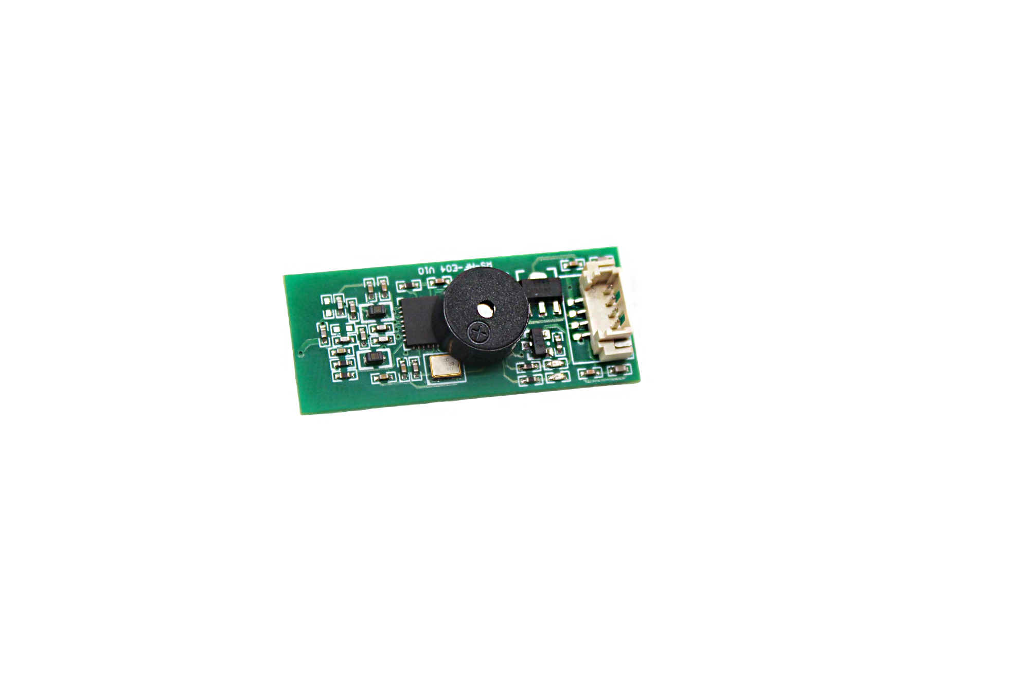
Even the most rigid gantry systems flex under acceleration. A pick-and-place head moving at several meters per second carries a tiny die, and the deceleration phase can introduce a lateral shift of a few microns if the vacuum nozzle's compliance is not perfectly balanced. Over thousands of placements, temperature changes in the linear motors and ball screws expand the frame just enough to move the nominal origin. What looks like a random scatter in final inspection is often a slow, repeatable drift tied to warm-up cycles and belt tension.
The real trouble starts when the vision system corrects for the wrong reference. If fiducial recognition locks onto a solder mask edge that shifts slightly between board batches, the machine will chase a phantom offset. Operators may see placement accuracy degrade only on certain panel quadrants, which points to local board support sag rather than a global calibration issue. Checking vacuum blow-off timing and nozzle tip wear usually recovers more microns than a full axis re-mapping, because the drift is rarely from the encoders alone.
Encapsulation Cracks That Invite Moisture Early
Encapsulation materials like epoxy resins often develop microcracks during thermal cycling or mechanical stress. These cracks act as capillary pathways, drawing moisture directly into the package interior long before any visible damage appears.
Once a crack forms, humid air can condense inside the cavity. Water molecules then react with metallic interconnects and the die surface, accelerating corrosion and delamination within the first few hundred hours of operation.
Even hairline fractures near the lead frame or die attach region permit enough moisture ingress to shift leakage currents. This early-stage intrusion degrades insulation resistance and can trigger intermittent failures that are difficult to trace back to the original encapsulation defect.
Why Some Tags Die in Cold Storage but Survive the Lab
A tag that reads reliably on a lab bench can fail within hours inside a walk-in freezer. The difference rarely comes from the chip itself. It comes from how the antenna and its housing react to moisture, frost, and rapid temperature swings. In a dry lab, the tag sits in stable air with a consistent dielectric environment. In cold storage, the moment a door opens, warm humid air rushes in and condenses on every surface, including the tag. That thin film of water, and later ice, changes the antenna's tuning just enough to push its response outside the reader's expected range. Passive UHF tags are especially vulnerable because they rely on a precise impedance match to harvest enough energy to reply.
Temperature cycling adds mechanical stress that static lab tests never reproduce. A tag bonded to a plastic crate or metal rack will expand and contract at a different rate than the substrate. Over days and weeks, tiny fractures form in solder joints or the antenna trace lifts away from its backing. Active tags face another issue: coin cell batteries lose voltage faster at low temperatures, so a tag that chirps happily at room temperature may go silent after a few cold hours. Meanwhile, condensation can corrode contacts or create a short across exposed terminals. These failures are cumulative and often occur only after the tag has been in service long enough to pass a short bench evaluation.
Then there is the problem of reading through frost-covered packaging and dense frozen product. Ice is not RF-friendly; it absorbs and scatters signals, and when an item is buried under stacks of frozen goods, the tag may be shielded by a wall of water in solid form. Lab tests usually isolate a single tag in open air, a few feet from the antenna. Real cold storage puts tags deep inside pallets, next to metal freezer racks, and behind plastic film that can develop its own charged condensation layer. If the tag survives electrically, it still has to overcome an environment that works against the signal at every layer. That is why field performance can diverge so sharply from laboratory promise.
Trimming Die Attach Costs Without Losing Yield
When die attach costs come under pressure, the usual move is to ask suppliers for a lower price on epoxy or solder. That rarely sticks, because the real waste sits in the dispense pattern. Many lines over-dispense by 10–20% simply to avoid starvation at the die edge. Mapping wetting behavior on the leadframe or substrate lets you tighten the pattern and cut material without shrinking the bond area. The qualified material stays the same, so yield does not move.
Placement force and dwell time can quietly eat into cost too. Too much force cracks thin die or squeezes out enough adhesive to create edge voids, both of which show up as yield loss or field returns. A short DOE around force and time often shows that a lower setting still produces full fillet coverage while reducing scrap and rework. The savings from fewer rejects usually outweigh anything you can get from hammering the material price.
Inline inspection data offers another way to hold costs down. Instead of periodic sampling, feed the measurements back to adjust dispense volume and placement position in real time. That prevents slow drift toward excess material or incomplete coverage. The result is lower ongoing spend through tighter control, not through untested substitutions, so yield stays flat or improves.
Reading Between the Layers: Delamination Stress Tests
Most laminate failures begin where nobody is looking. The surface stays intact while shear stresses quietly peel one ply from another, and by the time a crack becomes visible, the bond has already given up. Delamination stress tests are designed to catch that quiet failure early, measuring the force needed to split layers apart under controlled conditions.
A typical setup involves a pre-cracked specimen loaded in a way that encourages the crack to run between plies, not through them. Technicians watch how the crack tip moves, whether it stalls, jumps, or leaves behind a clean separation. The raw numbers matter less than the pattern of resistance: a steady climb suggests a tough interface, while a sudden drop points to uneven curing or contamination.
Reading these results is less about checking a pass/fail box and more about interpreting the story left on the fractured surfaces. Fibers pulled from the resin, resin smeared across fibers, or bare patches where no bonding occurred each tell a different tale. The test does not just quantify adhesion; it reveals the manufacturing history hidden inside the laminate.
FAQ
Most failures come down to stress on the chip connection. When the web runs fast, tension spikes can flex the inlay enough to crack the micro-weld between chip and antenna. Using a thicker, more dimensionally stable PET substrate and reducing nip pressure on the strap area helps a lot. Also, running a pull test after each roll change catches weak bonds before they become customer defects.
Read range variation usually points to inconsistent antenna geometry or uneven chip impedance matching. Instead of relying only on visual inspection, implement automated optical inspection that measures antenna width and gap at the tuning loop. Then run a sample of each batch on a benchtop RFID tester with the same fixture and orientation. Logging those readings over time lets you spot drift in etching or printing before it gets out of hand.
The trick is to avoid sharp thermal gradients and mechanical shock at the flip-chip bond. Using an anisotropic conductive paste rather than a rigid solder bump can absorb some of the stress. Also, preheating the substrate before bonding and then ramping temperature down gradually reduces micro-cracks in the chip die. Adding a low-force placement check after bonding with x-ray or acoustic imaging catches hidden cracks early.
For item-level tagging, silver ink is attractive but can get expensive. A good middle ground is using a thinner aluminum foil antenna with a fine line design that keeps conductivity acceptable. Copper is rarely needed unless you are dealing with very high frequencies or demanding read distances. Compare the cost per square meter including waste, not just raw material price, and run a small pilot on your actual converting line before committing.
On metal, the tag's antenna detunes because the conductive surface changes the field distribution. A thin foam or air gap spacer between the tag and the metal can shift the resonance back into range, but that adds thickness and cost. For a slimmer approach, design a tag with a ground-plane structure, like a patch antenna, or use a ferrite absorber layer. Prototype both options because the best choice depends heavily on the tag footprint and the type of metal object.
Intermittent failures are often caused by weak bonds or hairline cracks that only show under bending or temperature cycling. A practical QC flow is to run a sample from each production lot through a three-point flex test, then a thermal shock from -20C to 70C, and finally a read-write cycle on both sides of the tag. If even one tag in the sample loses performance or fails to encode, hold the lot. This catches problems that a simple static read test misses.
Rather than buying a full anechoic chamber, start with a portable RFID reader and a shielded enclosure made from RF absorber foam. That gives you repeatable near-field and mid-field measurements for a fraction of the price. Rent or share an anechoic chamber for periodic validation. Also, many tag chip vendors offer free or low-cost tuning guides and reference designs that include test fixtures, which reduces the need for custom gear.
Substrate choice is often the difference between a tag that survives one season and one that lasts five years. PET works for indoor use, but UV and moisture will degrade it outdoors. Switch to a UV-stabilized polycarbonate or a laminated film with an acrylic adhesive. For extreme conditions, use a ceramic substrate or encapsulate the inlay in epoxy. Always test the full tag stack—not just the inlay—in a QUV weathering chamber and a salt fog test if the tags will be near coastal areas.
Conclusion
RFID chip tag production faces a cluster of issues that often surface only after volume ramps. Thinner antenna traces can boost read range on paper, but real-world performance drops when conductivity paths narrow and stray capacitance shifts. Pick-and-place equipment may drift by just a few microns, yet that is enough to misalign the chip on the antenna pads, cutting coupling efficiency and raising failure rates. Encapsulation layers that cure too rigid or too thin develop hairline cracks almost immediately, letting moisture seep into the die attach area long before the tag leaves the factory floor. Tackling these means tightening process controls: laser-trimmed antenna geometries, vision-guided placement with sub-micron feedback, and encapsulant formulations that flex with thermal cycling rather than fighting it.
Cold storage failures are a classic example of lab validation missing field conditions. Tags that pass room-temperature reads can die at -25°C because the adhesive between chip and substrate becomes brittle or the antenna delaminates under contraction. Trimming die attach costs without sacrificing yield requires moving away from outdated conductive epoxies toward lower-cure anisotropic conductive films or precise jetting of smaller adhesive volumes—but only if bond strength is verified at temperature extremes. Delamination stress tests that mimic repeated freeze-thaw and humidity shocks expose weak interlayer adhesion early, letting manufacturers screen out batches before they ship. The overarching fix is not a single magic material; it is matching every process choice to the actual environmental envelope the tag will face.
Contact Us
Contact Person: Esme Mo
Email: [email protected]
Tel/WhatsApp: 0086 191 2931 7837
Website: https://www.osrfidglobal.com/